The areas of focus include studying materials with advanced microscopy tools and Defect Engineered Materials Design for developing high-performance materials tailored for defects.
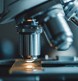
Advanced Microscopy and Materials
Materials form the basis for most of the technology advancements in every sphere of life. Such advanced materials that are being widely researched include multi-phase steels, high- temperature superalloys, high entropy alloys, 2D materials, semiconductor and electronic materials, multifunctional oxides, nitrides, and halides, energy storage and conversion materials, etc. The properties can be enhanced by designing and tailoring the microstructure to derive exotic functional and load-bearing properties. Towards this goal, it is essential to understand the scientific origin of the properties down to the atomic scale through microscopy tools.
Studying the materials with advanced microscopy tools has opened an opportunity to understand the structure and chemistry at the atomic scale. The best combination of electron optics, ultra-sensitive detectors ensure that even the lightest, most sensitive materials can be characterized at sub-angstrom scale. The aberration correction in the electron beam as a probe has enabled to obtain high-quality atomic-level chemical identity and bonding-state information in materials by simultaneous X-ray energy dispersive spectroscopy and electron energy loss spectroscopy (EELS). Atom probe tomography (APT) complements the above techniques with precise quantitative data at the atomic scale. Thus, a combination of the two techniques offers a unique state-of-the-art characterization in the field of materials research
Principal Investigator: S. Sankaran
Correlative Microscopy
Area of Focus – Defect Engineered Materials Design (DEMD):
Highlight: The centre of excellence (CoE) in “Defect Engineered Materials Design (DEMD)” intends to establish a unique facility namely, ‘Field Ion Microscope (FIM)’ that can image even individual atoms, custom designed and constructed to characterize zero-dimensional (0D) defects in materials. The envisaged FIM will be interconnected to complement other existing varied length-scale microscopy facilities such as Scanning and Transmission Electron Microscope ((S)TEM) which can image 1D, 2D and 3D defects along with near-atomic scale 3D elemental distribution and precise composition analysis capability of Atom Probe Tomography (APT). To this end, the centre intends to integrate and enrich the existing microscopy skill-sets together with computational expertise towards unravelling the unexplored territory of ‘Defect Engineered Materials Design’ for developing high-performance materials tailored for defects.
Principal Investigator: K. G. Pradeep